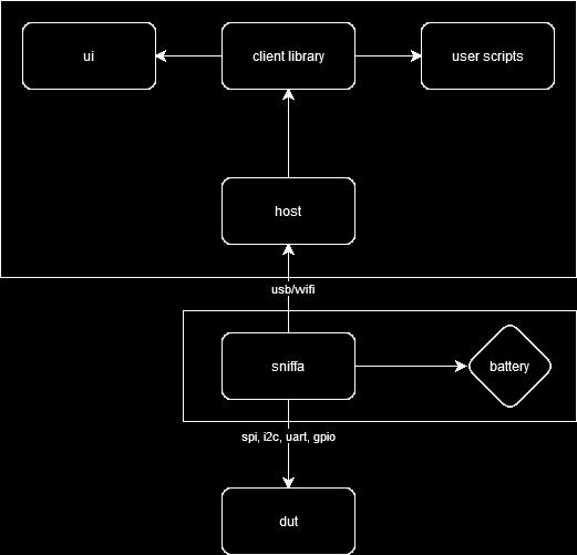
schematic (pset 3)
@carboxyl: this page is available on my blog if you're interested in following any of the hyperlinks: https://blog.npry.dev/class/smallmfg/market-research.
This problem set is intended to help you move towards a final electrical design, so PCBs can be made (if needed). Bring a hard copy to turn in during class on the due date.
- Please put together a schematic of what you intend to build, and a description of its various subcomponents (power, charging, battery, sensing, computation, UI, amplifiers, etc). Give rough estimates of important quantites (battery life, noise floor, sensitivity, processing time, etc). It is okay if your project will be made of dev- boards or other purchases subassemblies, but be sure to include how they will be interconnected and their performance attributes.
- Schedule a time to meet with me to discuss your project (~1h). We will go over where you are currently at, and how to best proceed.
schematic pdf (printed / attached to physical turnin)

block diagram
sniffa will be designed around a fabricated PCB with the following (major) components:
-
ESP32C6 microcontroller (WiFi, 802.15.4, BLE, USB, SPI, I2C, UART onboard)
- $3 in low quantities for the module with integrated flash
- High (<= 160MHz) and low (<= 20MHz) power cores
- 7 uA deep sleep, <1mA light sleep, 25mA modem sleep, 40mA (HP core), 300mA WiFi tx (active), 80mA WiFi rx (active)
- Full IO matrix
- Event/task matrix
- 21 available GPIOs
- 7 ADC lines
-
BQ25185DLHR: 1S LiPo battery regulator supporting VUSB charging with 4.5V regulated output
- ~$1 in quantity
- Supports up to 3A on the VSYS output
-
3V3 buck for the regulator^ VSYS output, rated for 1A -- dedicated to internal power
-
3V3 buck and 5V boost for external power, 1A each
-
LDO as stable ADC VREF
- Optional, analog monitoring is just a nice-to-have
-
5V level shifters
-
Battery (4000mAh, 1S): https://www.amazon.com/dp/B095HD7JCR, $17 -- aiming for at least 8h of runtime while powering a low-ish power (~ sensor node, no major actuation) device for testing, think this could be scaled back
Target performance is 40MHz SPI (slave + master), 1MHz I2C, 1MBaud UART with DMA. The esp32c6 can do all of these except I2C, which is capped at 400kHz, but it was the best tradeoff I could find (as it comes in a module and has integrated networking).
That's 5MB/s at full SPI rates, and I probably can't simultaneously get that performance out of the 2.4GHz WiFi connection, so there's a tradeoff to be made re: buffering that comes down to the practical distribution of traffic throughputs in normal use for the device, compared to WiFi link speed. Most of the usage profile I understand for a device like this is on the order of 1% link budget utilization or less — most projects simply don't need to read from a bus that often, and even when they do, it's not very much data per transaction. I estimate that a 64kB data buffer is probably way overkill here, and the ESP32C6 has 512kB of RAM, so there's plenty of margin on top of that.
I/O protection
I thought about a few ways to do protection on the I/Os — the usage model for a device like this should really account for users accidentally plugging arbitrary voltage into almost any exposed I/O line whether it should be there or not. Design limitations suggest that we should consider reasonable voltages for electronics projects -- being tolerant to kilovolts is unreasonable, and even mains is probably out of scope. But I think +/- 20V of ground is a reasonable tolerance range for small EE projects.
The easiest thing to do is slap TVS diodes on everything and call it a day. The design I initially considered was:
+ 3V3

   |

  TVS

   |

  SIG

   |

  TVS

   |

  GND
where each TVS is bidirectional with a breakdown at 3V3. The idea being that they would clamp the signal to within 0V -> 3V3. The problem with this approach is that I think it's unrealistic that a user would quickly notice something was plugged into the wrong place, and the diodes might have to sink a lot of current and so dissipate a lot of heat. As far as I know, TVS diodes aren't generally designed for this -- they're mostly meant to handle transients, so this is maybe not an ideal approach. I'm sure I could find diodes that could handle this, but this design feels hacky overall, so I thought about how else I could address this problem.
One possibility is cutting output power if a signal is detected out of range, but I don't want to rely on that either. I see output power as a convenience in the design, not a usage necessity.
I started thinking about a design using FETs with comparators as gate drivers, which I think would probably work, but realized that the behavior I want is isolation between the microcontroller side and the external ports — I think what I'm actually looking for is an optocoupler. Looking at digikey, I'm seeing about $1.50 per part with 4 channels (so BoM cost for me is $9 for 21 channels), but those parts are only unidirectional. I could live with this, as I don't really need 21 channels for the design intent of the project, but that's a somewhat pricy addition to the BoM. Many of these also have frequency limits that come up against my desired SPI rates -- I think 10MHz would be fine, but I'm seeing a lot of isolators that will only handle up to about 1MHz.
On course, there are some from ADI that are $10/unit and do bidirectional translation, but that's painfully expensive.